Diode
A diode is an electrical device allowing current to move through it in one direction with far greater ease than in the other. The most common kind of diode in modern circuit design is the semiconductor diode, although other diode technologies exist.
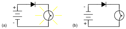
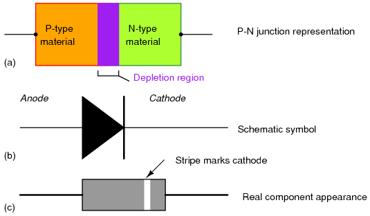
Here is the reason that makes diode directional. Modern semiconductor diode is made of a crystal of semiconductor like silicon that has impurities added to it to create a region on one side that contains negative charge carriers (electrons), called n-type semiconductor, and a region on the other side that contains positive charge carriers (holes), called p-type semiconductor. The diode's terminals are attached to each of these regions. The boundary within the crystal between these two regions, called a PN junction, is where the action of the diode takes place. The crystal conducts conventional current in a direction from the p-type side (called the anode) to the n-type side (called the cathode), but not in the opposite direction.
p-n junction
A p–n junction is formed by joining p-type and n-type semiconductors together in very close contact. The term junction refers to the boundary interface where the two regions of the semiconductor meet. If they were constructed of two separate pieces this would introduce a grain boundary, so p–n junctions are created in a single crystal of semiconductor by doping, for example by ion implantation, diffusion of dopants, or by epitaxy (growing a layer of crystal doped with one type of dopant on top of a layer of crystal doped with another type of dopant).
Properties Of a p-n junction
The p–n junction possesses some interesting properties which have useful applications in modern electronics. A p-doped semiconductor is relatively conductive. The same is true of an n-doped semiconductor, but the junction between them is a nonconductor. This nonconducting layer, called the depletion zone, occurs because the electrical charge carriers in doped n-type and p-type silicon (electrons and holes, respectively) diffuse into the other type of material (i.e. electrons in p-type and holes in n-type) and eliminate each other in a process called recombination. By manipulating this non-conductive layer, p–n junctions are commonly used as diodes: circuit elements that allow a flow of electricity in one direction but not in the other (opposite) direction. This property is explained in terms of forward bias and reverse bias, where the term bias refers to an application of electric voltage to the p–n junction.
Equilibrium (Zero Bias)
he p–n junction possesses some interesting properties which have useful applications in modern electronics. A p-doped semiconductor is relatively conductive. The same is true of an n-doped semiconductor, but the junction between them is a nonconductor. This nonconducting layer, called the depletion zone, occurs because the electrical charge carriers in doped n-type and p-type silicon (electrons and holes, respectively) diffuse into the other type of material (i.e. electrons in p-type and holes in n-type) and eliminate each other in a process called recombination. By manipulating this non-conductive layer, p–n junctions are commonly used as diodes: circuit elements that allow a flow of electricity in one direction but not in the other (opposite) direction. This property is explained in terms of forward bias and reverse bias, where the term bias refers to an application of electric voltage to the p–n junction.

Figure A
A p–n junction in thermal equilibrium with zero bias voltage applied. Electrons and holes concentration are reported respectively with blue and red lines. Gray regions are charge neutral. Light red zone is positively charged. Light blue zone is negatively charged. The electric field is shown on the bottom, the electrostatic force on electrons and holes and the direction in which the diffusion tends to move electrons and holes.
The electric field created by the space charge region opposes the diffusion process for both electrons and holes. There are two concurrent phenomena: the diffusion process that tends to generate more space charge, and the electric field generated by the space charge that tends to counteract the diffusion. The carrier concentration profile at equilibrium is shown in figure A with blue and red lines. Also shown are the two counterbalancing phenomena that establish equilibrium.

Figure B
A p–n junction in thermal equilibrium with zero bias voltage applied. Under the junction, plots for the charge density, the electric field and the voltage are reported.
The space charge region is a zone with a net charge provided by the fixed ions (donors or acceptors) that have been left uncovered by majority carrier diffusion. When equilibrium is reached, the charge density is approximated by the displayed step function. In fact, the region is completely depleted of majority carriers (leaving a charge density equal to the net doping level), and the edge between the space charge region and the neutral region is quite sharp (see figure B, Q(x) graph). The space charge region has the same charge on both sides of the p–n interfaces, thus it extends farther on the less doped side (the n side in figures A and B).
The space charge region is a zone with a net charge provided by the fixed ions (donors or acceptors) that have been left uncovered by majority carrier diffusion. When equilibrium is reached, the charge density is approximated by the displayed step function. In fact, the region is completely depleted of majority carriers (leaving a charge density equal to the net doping level), and the edge between the space charge region and the neutral region is quite sharp (see figure B, Q(x) graph). The space charge region has the same charge on both sides of the p–n interfaces, thus it extends farther on the less doped side (the n side in figures A and B).
Forward Bias
With a battery connected this way, the holes in the P-type region and the electrons in the N-type region are pushed towards the junction. This reduces the width of the depletion zone. The positive charge applied to the P-type material repels the holes, while the negative charge applied to the N-type material repels the electrons. As electrons and holes are pushed towards the junction, the distance between them decreases. This lowers the barrier in potential. With increasing forward-bias voltage, the depletion zone eventually becomes thin enough that the zone's electric field can't counteract charge carrier motion across the p–n junction, consequently reducing electrical resistance. The electrons which cross the p–n junction into the P-type material (or holes which cross into the N-type material) will diffuse in the near-neutral region. Therefore, the amount of minority diffusion in the near-neutral zones determines the amount of current that may flow through the diode.

Only majority carriers (electrons in N-type material or holes in P-type) can flow through a semiconductor for a macroscopic length. With this in mind, consider the flow of electrons across the junction. The forward bias causes a force on the electrons pushing them from the N side toward the P side. With forward bias, the depletion region is narrow enough that electrons can cross the junction and inject into the P-type material. However, they do not continue to flow through the P-type material indefinitely, because it is energetically favorable for them to recombine with holes. The average length an electron travels through the P-type material before recombining is called the diffusion length, and it is typically on the order of microns.
Although the electrons penetrate only a short distance into the P-type material, the electric current continues uninterrupted, because holes (the majority carriers) begin to flow in the opposite direction. The total current (the sum of the electron and hole currents) is constant in space, because any variation would cause charge buildup over time (this is Kirchhoff's current law). The flow of holes from the P-type region into the N-type region is exactly analogous to the flow of electrons from N to P (electrons and holes swap roles and the signs of all currents and voltages are reversed).
Therefore, the macroscopic picture of the current flow through the diode involves electrons flowing through the N-type region toward the junction, holes flowing through the P-type region in the opposite direction toward the junction, and the two species of carriers constantly recombining in the vicinity of the junction. The electrons and holes travel in opposite directions, but they also have opposite charges, so the overall current is in the same direction on both sides of the diode, as required.
Reverse Bias
Reverse biased usually refers to how a diode is used in a circuit. If a diode is reverse biased, the voltage at the cathode is higher than that at the anode. Therefore, no current will flow until the diode breaks down. Connecting the P-type region to the negative terminal of the battery and the N-type region to the positive terminal, corresponds to reverse bias. The connections are illustrated in the following diagram:
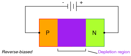
Because the p-type material is now connected to the negative terminal of the power supply, the 'holes' in the P-type material are pulled away from the junction, causing the width of the depletion zone to increase. Similarly, because the N-type region is connected to the positive terminal, the electrons will also be pulled away from the junction. Therefore the depletion region widens, and does so increasingly with increasing reverse-bias voltage. This increases the voltage barrier causing a high resistance to the flow of charge carriers thus allowing minimal electric current to cross the p–n junction.
The strength of the depletion zone electric field increases as the reverse-bias voltage increases. Once the electric field intensity increases beyond a critical level, the p–n junction depletion zone breaks-down and current begins to flow, usually by either the Zener or avalanche breakdown processes. Both of these breakdown processes are non-destructive and are reversible, so long as the amount of current flowing does not reach levels that cause the semiconductor material to overheat and cause thermal damage.
Here are the sources I compiled the information from,
Wikipedia Diode - http://en.wikipedia.org/wiki/Diode
Wikipedia p-n junction - http://en.wikipedia.org/wiki/P-n_junction
allaboutcircuits - http://www.allaboutcircuits.com/vol_3/chpt_3/1.html
No comments:
Post a Comment